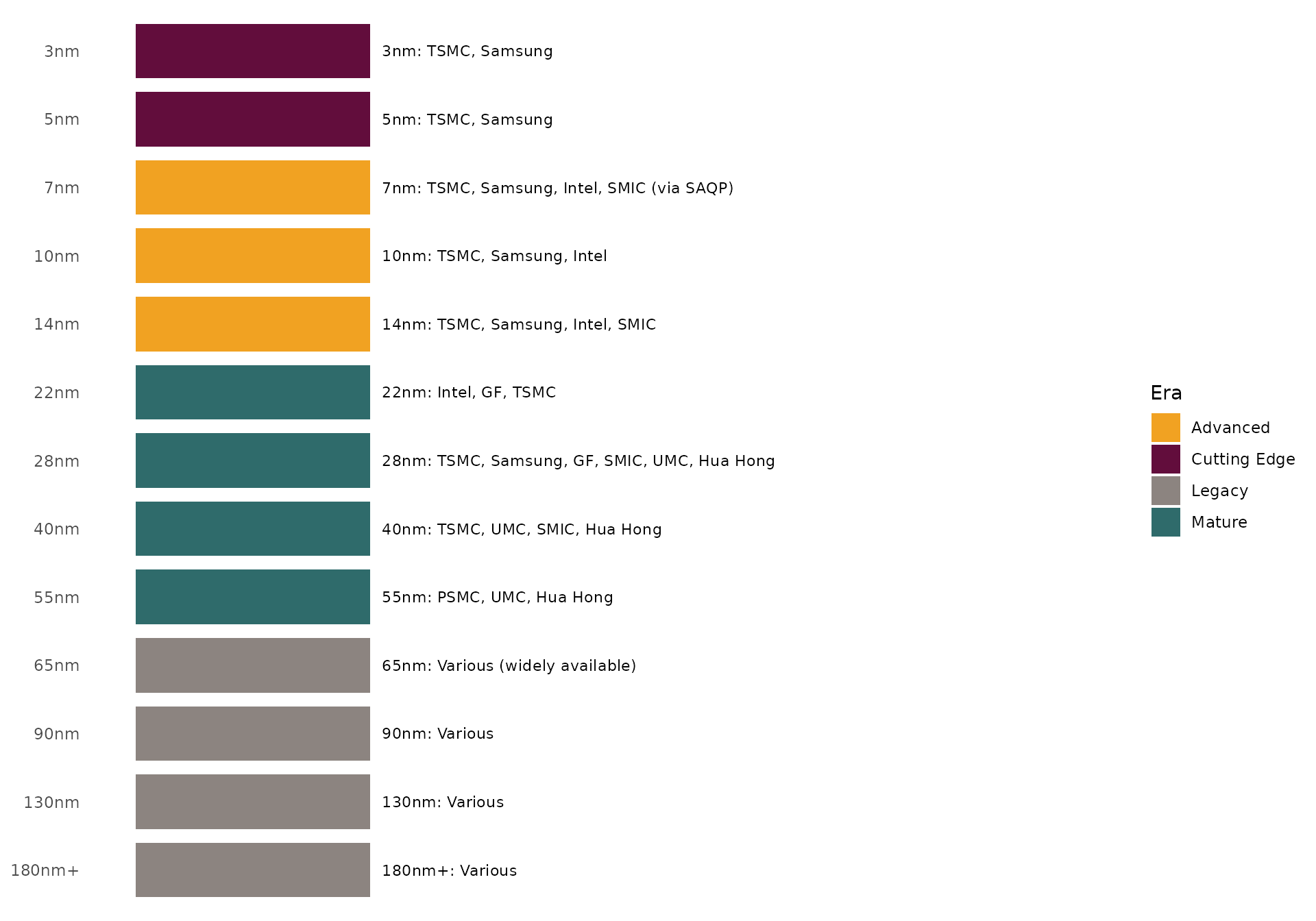
Technology Nodes
China’s process-node trajectory under export controls
China’s process-node trajectory under export controls — every tracked facility, from 180nm legacy to N+1/N+2 leading-edge attempts.
The Global Node Landscape
Semiconductor “nodes” refer to manufacturing process technology; smaller numbers generally mean more advanced chips.
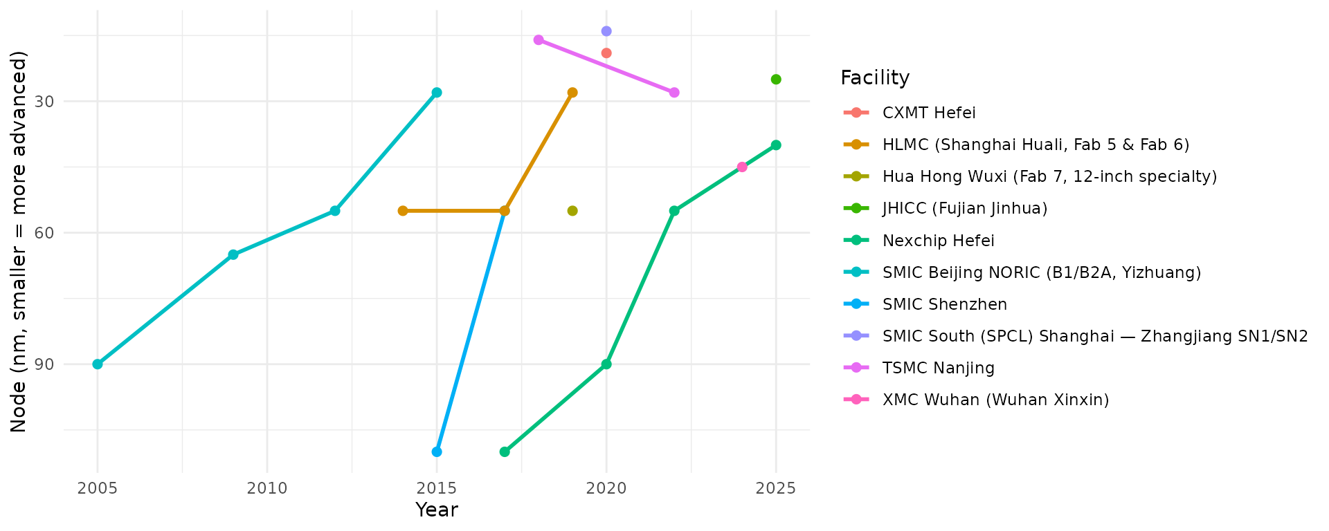
China’s Indigenization Trajectory
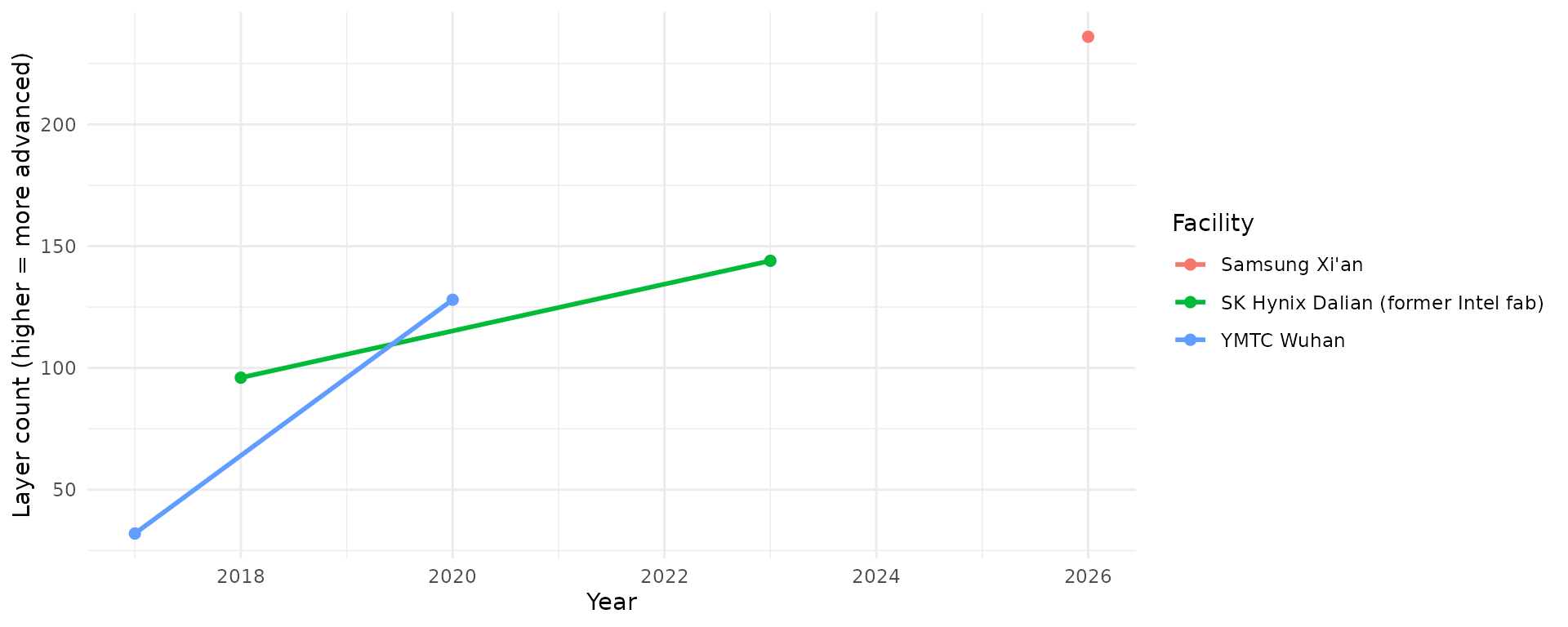
Each line traces one facility’s most advanced disclosed process technology over time — the clearest signal of how effectively export controls have slowed (or failed to slow) specific fabs. Logic/DRAM process width (nm) and 3D NAND layer count are different units and are never plotted on the same axis — a higher layer count is more advanced, while a smaller nm figure is more advanced, so combining them on one chart would misread as a regression for exactly the facilities making the fastest progress.
Logic / DRAM Process Width
3D NAND Layer Count
NoteReading These Charts
A facility with no plotted line has not yet had its node history researched (see About for data status). Absence from a chart is a data gap, not a claim about the facility’s capability. An entry whose process technology doesn’t parse into either unit (for example, a named-but-unquantified node such as “DDR5-capable, exact width not disclosed”) is excluded from both charts rather than guessed — it still appears in that facility’s own profile page.
Monthly Wafer Capacity
Recorded monthly wafer starts for each fab, by wafer size. Capacity is shown only where a cited source gives a facility-specific figure. Bars are coloured by whether the figure is installed capacity or a planned/full-build target, since announced targets often run well ahead of what is actually running.
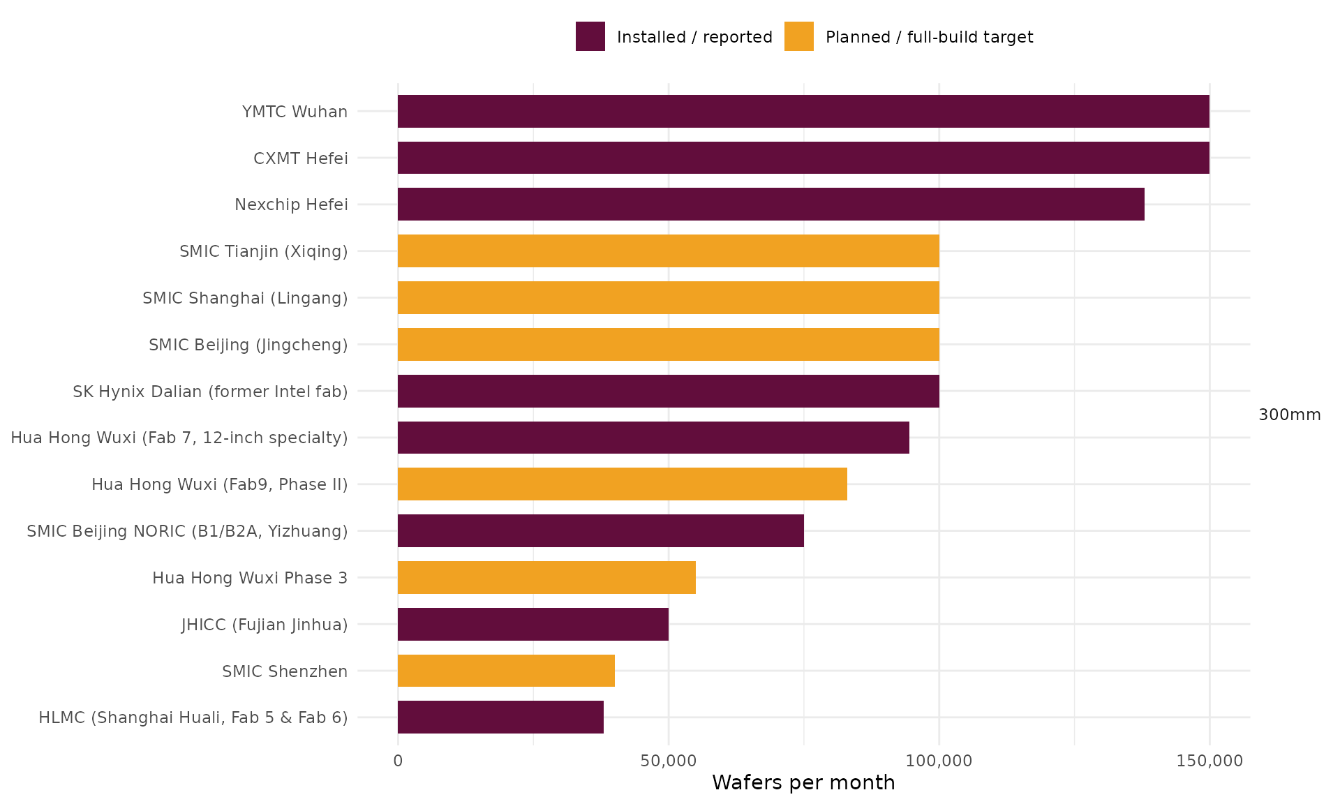
Wafer counts at different sizes are not comparable one-for-one: a 300mm wafer has about 2.25 times the area of a 200mm wafer. They are therefore shown in separate panels and never summed.
Advanced Packaging (OSAT Sites)
Assembly-and-test sites have no process node. Their equivalent is the packaging technology they can produce in volume, which matters more as chiplets and stacked memory let packaging make up for restricted lithography.
| Facility | Latest technology in production | Since | Capacity |
|---|---|---|---|
| JCET Jiangyin | company-wide: XDFOI chiplet (2.5D/3D fan-out) stable volume; 4nm MCM ship | 2023 | Not yet recorded |
| Tongfu Microelectronics Nantong | Nantong Chongchuan HQ: 8/12in wafer-level (Cu pillar, bump, WLCSP), as of | 2026 | 116,700,000 units/month, as of 2025 — theoretical capacity of the HPC/communications packaging business run by 南通通富 (Sutong plant): ~14亿块/yr / 12 = ~116.7M units/month; 2025 utilisation 78.88%. Not total Nantong capacity |
| Huatian Technology Tianshui | Tianshui: MCM/MCP multi-chip packaging expansion completed (18亿只/yr design) | 2024 | 150,000,000 units/month, as of 2024-12 — design capacity ADDED by the Tianshui MCM(MCP) project only (18亿只/yr / 12 = 150M units/month), completed end-2024; not total Tianshui site output |
| Intel Chengdu | Wafer pre-processing + advanced packaging + test (stated, as of) | 2026 | Not yet recorded |
| SK Hynix Chongqing (Assembly & Test) | Phase 2 dedicated packaging plant; phase 1 becomes test-only (planned) | 2019 | Planned: 167,000,000 units/month, as of 2019 — planned post-phase-2 capacity: ‘接近20亿只’/yr / 12 = ~167M units/month; phase 1 alone was ~9.6亿只/yr (~80M/month, matching the 2014 figure) |